The noise is still the time-averaged noise over the period as it appears at the output of the sampler. 2 Table of Contents Types of Jitter Random Jitter Deterministic Jitter Correlated and Uncorrelated Jitter.
2
Jitter Due to variation in control voltage Due to uncertainty involved in.
. This works by adding an ideal sampler at the output of the circuit and then observing the noise at that instant in time. Free-form general-purpose topology exploration. The trouble is that its quite hard to tell by looking at the waveform data alone whether it is deterministic or random jitter.
Integrated circuit building blocks. Simply run a transient analysis and after the PLL is locked apply the eye diagram function form the calculator in cadence. Oscillator Simulation on Cadence 6.
Serial links with an emphasis on SerDes channels. The eye diagram resulting from the time domain simulation is wide open and the 4-level signal can be clearly seen. The wide area in the eye diagram is the peak to peak jitter.
Or with wavescsanviva you can double-click on the x-axis and setup the eye diagram that way. Do tran analysis first to estimate the VCO frequency at the fixed Vctrl as the Beat frequency. Subscribe to our newsletter for the latest updates.
By analysis of circuit and EDA simulation the. Source-synchronous for parallel buses. In this case youd just see a single spread of data whereas if you read the documentation it explains that for the deterministic component it is looking for two peaks around each edge - so there would be some distribution due to the deterministic part.
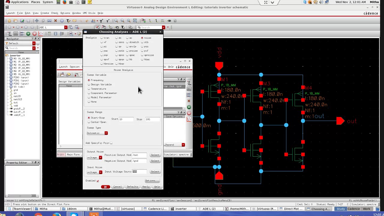
To help you quickly implement general topologies and standard interfaces Cadence Sigrity Advanced SI technology performs automated die-to-die signal integrity SI analysis in multiple modes. In this tutorial the procedure for doing noise analysis in ADEL is explained. Jitter is usually a time domain term while phase noise is a frequency domain term.
Jitter mode at least the pmjitter mode uses the time domain noise feature of pnoise analysis. Timing Jitter Tutorial Measurement Guide Silicon Labs Timing. PM jitter is a random fluc-tuation in the delay between the input an d the output events.
Very primary tutorial for cadence. Another way to get jitter is by the eye diagram. There are various random sources in ahdlLib - eg.
Start System requirement Statistical analysis include process mismatch effects. All parameter sets to their. 31 PM Jitter PM jitter is a non-accumulating jitter exhibited by driven systems.
Cadence simulation setup Monte Carlo Typical Model File Process Section 1. Based on standard 035 um5 v CMOS process model the circuit is simulated with Cadence EDA software. The Eye Diagram assistant in IC615 onwards gives the option of computing various metrics such as the standard deviation of the edge but if you need more general calculations you can use the SKILL code in solution 11395772.
Phase noise and jitter in digital electronics are unavoidable but you can design to minimize things like power dropout crosstalk reflections and EMI susceptibility with a complete set of system analysis tools from Cadence. Understanding EYE BER and BATHTUB Plots from DDR4 System. In the PLL the PFD CP and FDs all exhibit PM jitter.
Moreover a brief overview of the eye diagram is given. In these components an output event occurs as a direct result of and some time after an input event. This tutorial explains the procedure for plotting an eye diagram in Cadence.
ECE4902 Introduction to Analog IC Design is an undergraduate level course offered WPI which introduces students to the design and analysis of analog integrated circuits such as operational amplifiers phase-locked loops and analog multipliers. Archive over 14 years ago. Just run a transient simulation and then use the eyeDiagram function in the calculator to plot the eye diagram.
The Level 0 and Level 1 areas can be annotated by checking the Annotate check box. Hi im trying to plot the eye diagram of a jitter affected data using cadence spectre. This tutorial demonstrates the procedure for Post-layout simulations in Cadence and finding the number of parasitics in our layout.
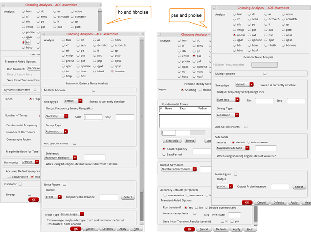
CADENCE Design Tools in ECE Undergraduate Courses. KVCO simulation PSS Periodic Steady State Analysis Any Verilog-A models are not allowed in the simulation bench PSS does not support Verilog-A. Unfortunately abs_jitter will only work with a periodic signal not with a random bit stream.

Cse 493 593 Cadence Tutorial
Measurement Of Phase Noise In Oscillators Rf Design Cadence Blogs Cadence Community
Cadence Ic615 Virtuoso Tutorial 9 Noise Analysis In Cadence Adel Youtube
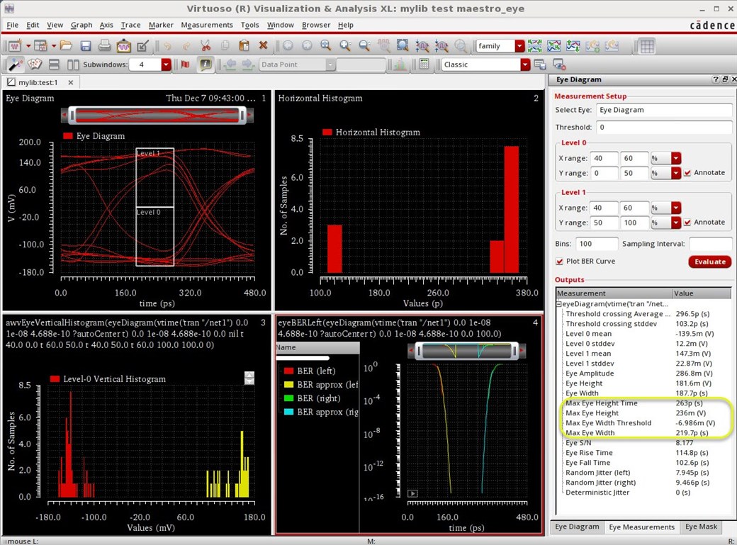
Virtuosity New Eye Diagram Measurements Custom Ic Design Cadence Blogs Cadence Community
2
2

Cadence 6 Tutorial 3 Youtube
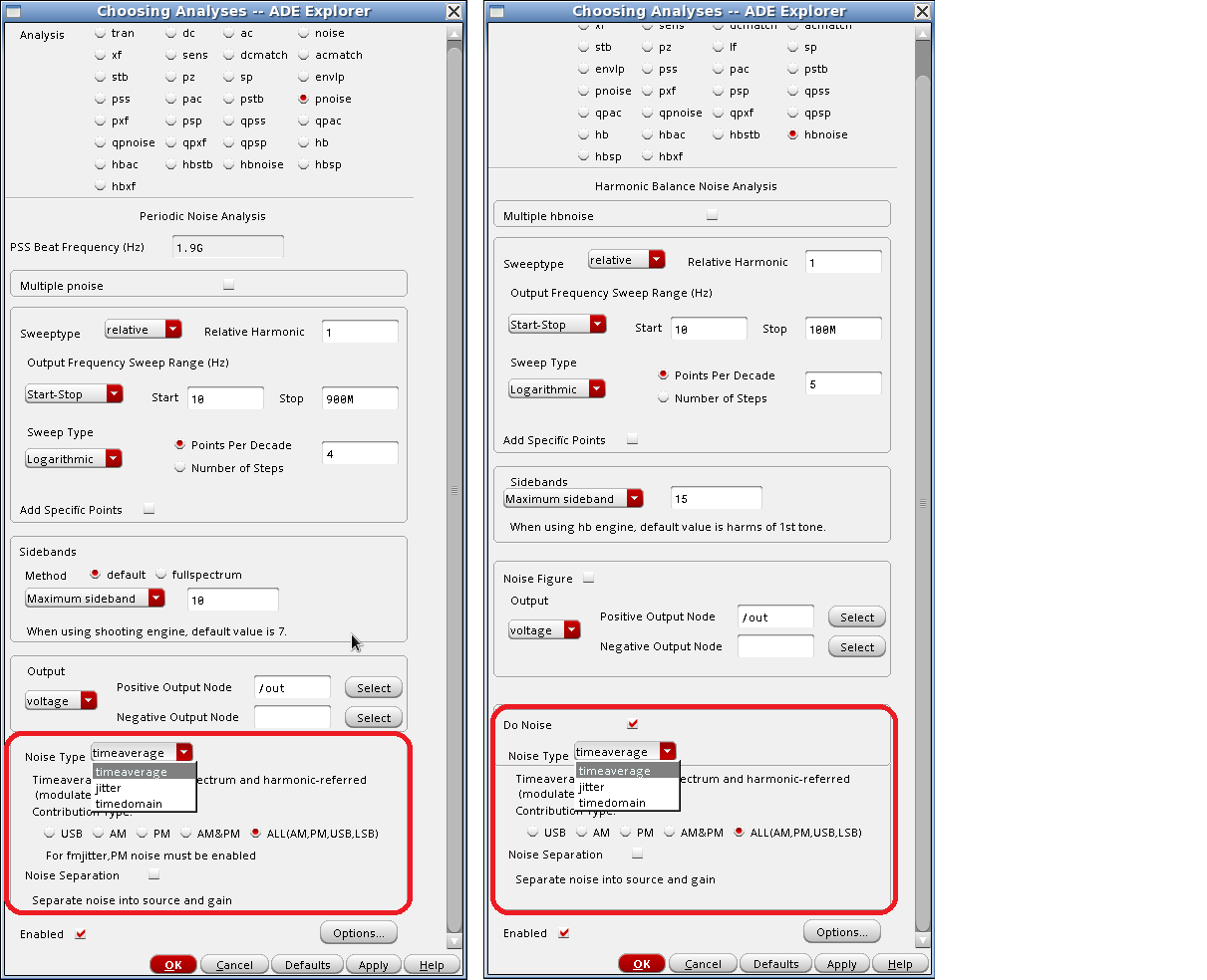
Noise Simulation In Spectre Rf Using Improved Pnoise Hbnoise And Direct Plot Form Options Rf Design Cadence Blogs Cadence Community
0 comments
Post a Comment